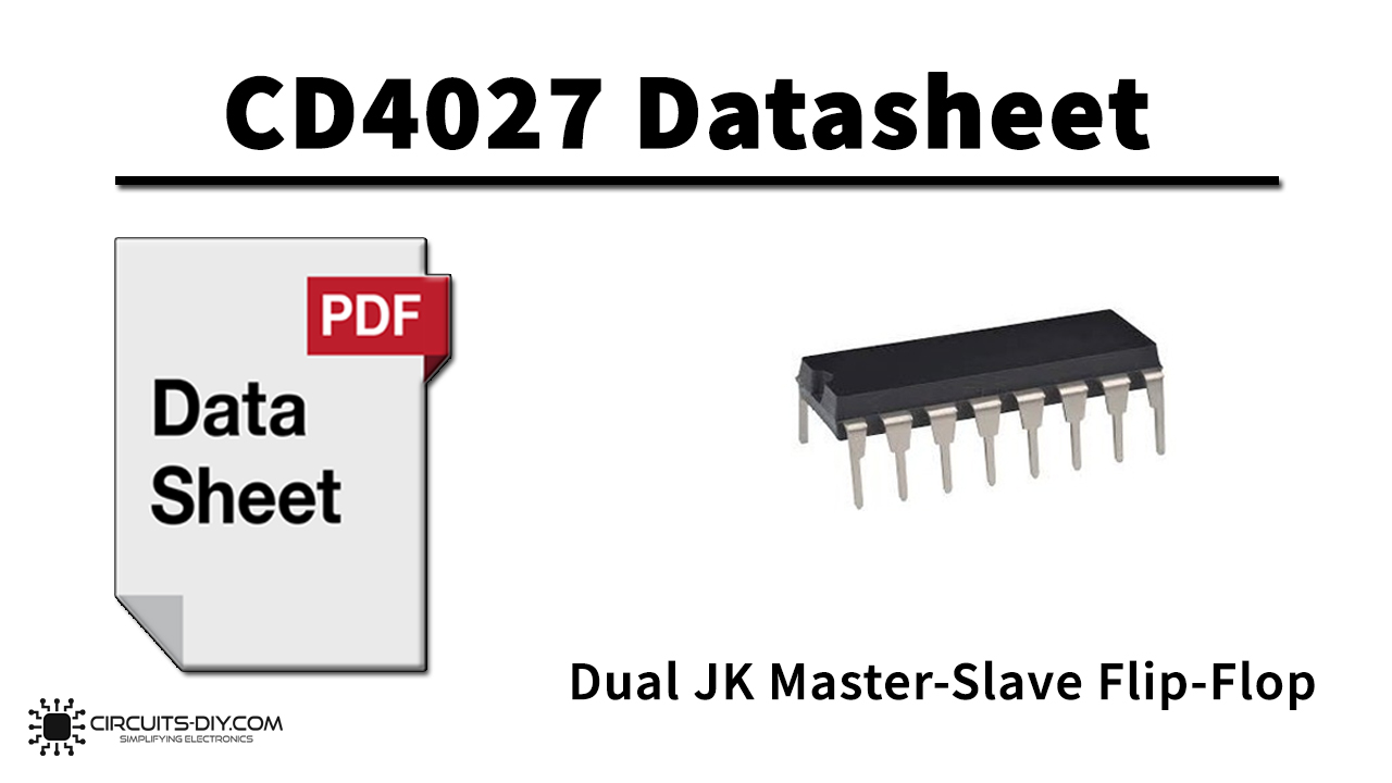
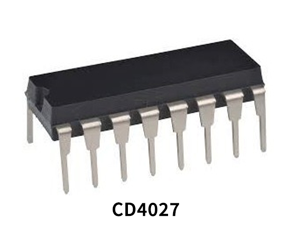
CD4027 belongs to the CD4XXX IC series. The IC is constructed by using the monolithic complementary MOS (CMOS), integrated with p-type and n-type enhancement mode transistors. Each flip-flop has independent J, K, set, reset, and clock inputs and buffered Q and Q outputs. These flip-flops are edge sensitive to the clock input and change state on the positive-going transition of the clock pulses. Set or reset is independent of the clock and is accomplished by a high level on the respective input. The output of the IC always comes in TTL and is directly interfaceable with other TTL, CMOS, and NMOS devices. The IC offers many features such as high noise immunity and low thermal dissipation. All inputs are protected against damage due to static discharge by diode clamps to VDD and VSS.
What is a JK Flip-Flop?
The JK Flip Flop is basically a gated RS flip flop with the addition of the clock input circuitry. When both the inputs S and R are equal to logic “1”, the invalid condition takes place. Thus to prevent this invalid condition, a clock circuit is introduced. The JK Flip Flop has four possible input combinations because of the addition of the clocked input. The four inputs are “logic 1”, ‘logic 0”. “No change’ and “Toggle”.
CD4027 Key Features
- Wide supply voltage range 3.0V to 15V
- High noise immunity 0.45 VDD (typ.)
- Low power TTL compatibility Fan out of 2 driving 74L or 1 driving 74LS
- Low power 50 nW (typ.)
- Medium speed operation 12 MHz (typ.) with 10V supply
CD4027 Pinout

| Pin No | Pin Name | Description |
|---|---|---|
| 1 | Q2 | output 0f flip flop 2 |
| 2 | Q2′ | complement output 0f flip flop 2 |
| 3 | CLK 2 | clock 2 signal |
| 4 | R2 | reset 2 value |
| 5 | K2 | input 1 of flip flop 2 |
| 6 | J2 | input 2 of flip flop 2 |
| 7 | SET 2 | set value 2 signal |
| 8 | VSS | source supply |
| 9 | SET 1 | set value 1 signal |
| 10 | J1 | input 1 of flip flop 1 |
| 11 | K1 | input 2 of flip flop 1 |
| 12 | R1 | reset 1 value |
| 13 | CLK 1 | clock 1 signal value |
| 14 | Q1′ | complement output 0f flip flop 1 |
| 15 | Q1 | output 0f flip flop 1 |
| 16 | VDD | Drain supply |
Application
- Shift Registers
- Ripple Binary Counters
CD4027 Datasheet
You can download the datasheet for CD4027 Dual JK Master-Slave Flip-Flop IC from the link given below:
See Also: CD4067 16-channel Analog Multiplexer/Demultiplexer Datasheet | CD40193 8-bit Up/Down Binary Counter – Datasheet | CD4502 Strobed Hex Inverter/Buffer – Datasheet

