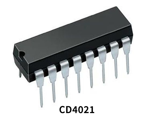
CD4021 belongs to the CD4000 IC series. CD4021 is an 8-stage parallel input/serial output shift register. A parallel/serial control input enables individual JAM inputs to each of the 8 stages. All outputs have equal source and sink current capabilities and conform to standard “B” series output drive. When the parallel/serial control input is in the logical “0” state, data is serially shifted into the register synchronously with the positive transition of the clock. When the parallel/ serial control is in the logical “1” state, data is jammed into each stage of the register asynchronously with the clock. The IC is always available in a 16 – pin hermetically sealed dual in line IC packaging (DIP), making it easy to use with TTL, CMOS, and NMOS devices. CD4021 offers many different features such as high noise immunity, ESD protection, and low power dissipation.
What is a Static Shift Register?
Static Shift registers are digital memory circuitry found in devices such as calculators, computers, and data processing systems. With a static shift register, data or bits are entered into the system in a serial or parallel manner. data entry is done from one direction, and as more data is added, it shifts positions until the data gets to the output end. The two ends are referred to as the left and right end. Movement of data can be from left to right, from right to left, or in both directions to make a bidirectional register.
CD4021 Key Features
- Wide supply voltage range: 3.0V to 15V
- High noise immunity: 0.45 VDD (typ.)
- Low power TTL compatibility: Fan out of 2 driving 74L or 1 driving 74LS
- 5V–10V–15V parametric ratings
- Symmetrical output characteristics
- Maximum input leakage 1 µA at 15V over full temperature range
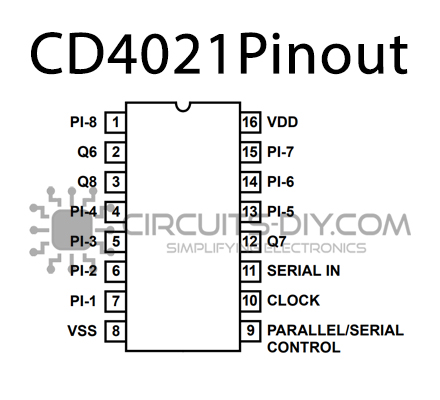
CD4021 Pinout
| Pin No | Pin Name | Description |
|---|---|---|
| 1 | P8 | Parallel Input 8 of Shift Register |
| 2 | Q6 | The output of Shift Register 6 |
| 3 | Q8 | The output of Shift Register 8 |
| 4 | P4 | Parallel Input 4 of Shift Register |
| 5 | P3 | Parallel Input 3 of Shift Register |
| 6 | P2 | Parallel Input 2 of Shift Register |
| 7 | P1 | Parallel Input 1 of Shift Register |
| 8 | GND | ground |
| 9 | LATCH | Latch Input |
| 10 | CLK | Clock Signal Input |
| 11 | SERIAL | Serial Input |
| 12 | Q7 | The output of Shift Register 7 |
| 13 | P5 | Parallel Input 5 of Shift Register |
| 14 | P6 | Parallel Input 6 of Shift Register |
| 15 | P7 | Parallel Input 7 of Shift Register |
| 16 | VDD | Drain Supply |
Application
- Parallel Input/Serial Output Data Queuing
- Parallel-to-Serial Data Conversion
- General-Purpose Register
CD4021 Datasheet
You can download the datasheet for CD4021 8-stage Static Shift Register from the link given below:
See Also: CD4543 BCD to 7-Segment Decoder – Datasheet | CD4584 Hex Schmitt Trigger – Datasheet | CD4553 3-Digit BCD Counter – Datasheet


