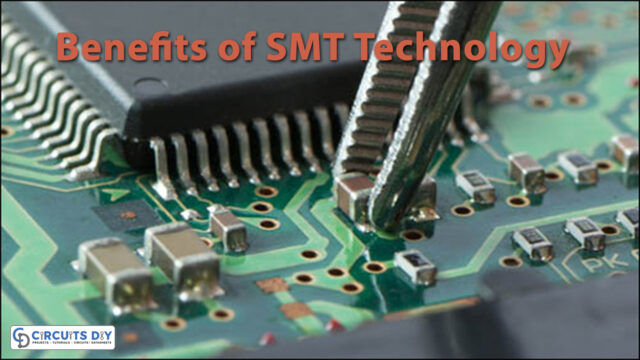
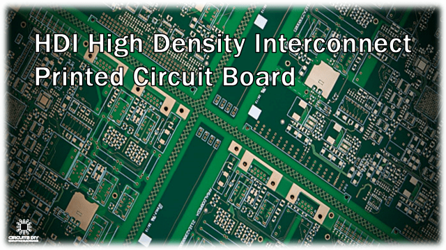
Surface mount technology is a domain of electronic PCB assembly in which SMD components are mounted on the surface of the PCB and then soldered, as opposed to the THT or through hole technology in which PCB board is drilled with holes for the components to be soldered. Surface mount technology was developed to reduce manufacturing costs and also to make more efficient use of PCB space. SMT has now made it possible to build highly complex PCBs into small scale assemblies with good replicability due to the higher level of automation. So, Today we will take a deep look into the SMT PCB Assembly Process & will cover each step that goes into the production and assembly of SMT PCBs.
What is SMT PCB Assembly Process?
SMT PCB Manufacturing and assembly is simply a structured chain process in which electronic PCBs are assembled by the use of automatic machines that place the SMD parts on the surface of the PCB. SMT PCB manufacturing & assembly does not only includes placing and soldering of components but also a wide array productions. All of which we shall be discussing in this comprehensive guide, in order to provide you with a complete outlook on the SMT PCB manufacturing process.
Surface Mount PCB Manufacturing Process

1) PCB Design & Layout Phase
The first phase of SMT PCB manufacturing starts in the design and layout phase of the PCB. In this stage, we basically work on the initial layout of the SMT PCB by using CAD software packages such as EasyEDA or EagleCAD.

2) Preparing Gerber/CAD To Centroid/ Pick & Place Files
Once the design and layout of the initial PCB is complete. The next step in the SMT PCB assembly is to prepare the essential PCB files to ensure that the process runs smoothly and to set up various machines used with the manufacturing process. Some of the important file for SMT PCB manufacturing are as following:
Gerber Files
Gerber File has info on your PCB such as PCB layout information, Layer information, spacing information, tracks to name a few.
BoM File
Bill Of Material (BoM) contains the list of all components in the PCB Layout.
CPL/PNP File
CPL/PNP file (Component Placement List/Pick & Place File). SMT Assembly machines need this file to determine where each part should be placed on the board.
3) PCB Material Examination & Stencil Preparation
In this stage, an examination of the SMC and the PCB determines whether there are any flaws in the PCB design. In conjunction with material evaluation, the PCB stencil is also prepared in this step. The stencil provides a fix position for solder paste printing. Technicians produce it with respect to the position of the solder pads in the SMT PCB design.
4) Solder Paste Printing
In solder paste printing process, the solder paste (usually a mixture of flux and tin) connects the SMC and solder pads on the PCB by the help of the stencil and squeegees. This is the most common method for solder paste printing but jet printing is also becoming very popular for large scale SMT operations.

5) SMC Part Placement
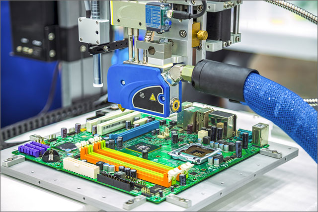
The printed & SPI inspected PCBs then move on to the next part of the manufacturing process which is the mounting of the SMC parts. Many factory SMT PCB operations utilize pick and place machines, which pick and place components with the help of vacuum or gripper nozzle and place them in the pre-programmed locations at high speed. After this, the PCB goes through a pre-reflow AOI (automated optical inspection) machine to verify that there are no mistakes in the Pick and place process and that all parts are in correct places before reflow soldering.

6) Reflow Soldering
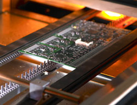
After component mounting and inspection, the SMT PCB boards move on to the reflow soldering process where a machine forms all the electrical solder connections between the SMC parts and the PCB by heating the entire assembly to a sufficient temperature. A reflow soldering machine consists of following stages:
- Soldering oven: After placing the SMC parts, the board goes into the reflow soldering oven.
- Pre-heat zone: the first part of a reflow soldering oven is the pre-heat zone, where the temperature of the board and all the components goes up simultaneously and gradually. The temperature variance rate in this section is 1.0℃ – 2.0℃ per second until it reaches 140℃ – 160℃.
- Soaking Phase: After preheating the boards remain in a soaking phase of the reflow oven between temperature from 140℃ – 160℃ for 60 – 90 secs.
- Reflow zone: the PCBs then enter a zone where the temperature increases at 1.0℃ – 2.0℃ per second to the peak of 210℃ – 230℃ to melt the tin in the solder paste, bonding the component leads to the pads on the PCB. The surface tension of the molten solder helps keep the components in place.
- Cooling zone: This section ensures that the solder freezes at the exit of the heating zone to avoid joint defects.
7) Post-Reflow AOI
After finishing the reflow soldering process, the boards go through another AOI inspection to ensure that no mistakes were done in the reflow soldering process & to determine that the solder joint quality is adequate.

8) Cleaning the Finished Board
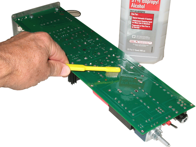
In the last step, the finished SMT PCB board is cleaned using iso-propyl alcohol wipes to remove any residual flux from the PCB board.
