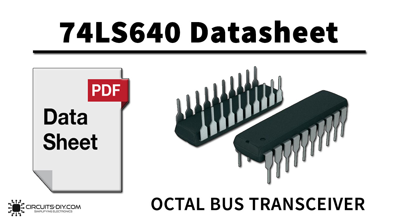
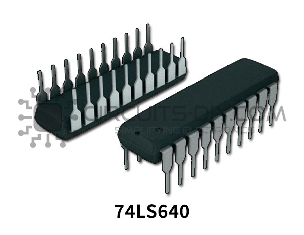
74LS640/74F640 IC is an octal transceiver featuring inverting 3-state bus compatible outputs. The 74F640/74LS640 bus transceivers are designed for asynchronous two-way communication between data buses. The devices transmit data from the A bus to the B bus or from the B bus to the A bus depending upon the level at the direction control (DIR) input. The enable input (G) can be used to disable the device so the buses are effectively isolated. The 74LS6407/4F640 IC has a vast array of working voltage, a wide range of working conditions, and directly interfaces with CMOS, NMOS, and TTL, which allows it to be used in high speed, low noise applications.
What is a Bus Transceiver Circuit?
Bus transceiver circuits are simple electronic tri-state, bi-directional devices that allow the flow of data between two points, making them compatible with bus-oriented systems or the bi-directional (input or output) control of any interface circuitry. A Bus transceiver can be inverting or non-inverting, common examples are 74LS243 & LS242 IC series. They are designed for asynchronous two-way communication between two data buses or input/output devices. The transceiver allows for the transmission of data from the terminal A to terminal B and vice versa depending on the logic level at the direction-control input.
74LS640/74F640 Pinout
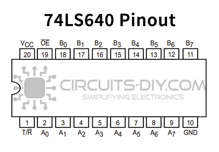
74LS640 Pin Configuration
| Pin No | Pin Name | Description |
|---|---|---|
| 1 | T/R’ | Transmit/Receive input For directional control (DIR) |
| 2 | A0 | Data (I/O) pin, Port A0 |
| 3 | A1 | Data (I/O) pin, Port A1 |
| 4 | A2 | Data (I/O) pin, Port A2 |
| 5 | A3 | Data (I/O) pin, Port A3 |
| 6 | A4 | Data (I/O) pin, Port A4 |
| 7 | A5 | Data (I/O) pin, Port A5 |
| 8 | A6 | Data (I/O) pin, Port A6 |
| 9 | A7 | Data (I/O) pin, Port A7 |
| 10 | GND | Ground Pin |
| 11 | B7 | Data (I/O) pin, Port B7 |
| 12 | B6 | Data (I/O) pin, Port B6 |
| 13 | B5 | Data (I/O) pin, Port B5 |
| 14 | B4 | Data (I/O) pin, Port B4 |
| 15 | B3 | Data (I/O) pin, Port B3 |
| 16 | B2 | Data (I/O) pin, Port B2 |
| 17 | B1 | Data (I/O) pin, Port B1 |
| 18 | B0 | Data (I/O) pin, Port B0 |
| 19 | OE’ | Active Low Output Enable Input |
| 20 | Vcc | Chip Supply Voltage |
74LS640/74F640 Features & Specifications
- Technology Family: f
- VCC (Min) (V) 4.75
- VCC (Max) (V) 5.25
- Bits (#) 8
- Voltage (Nom) (V) 5
- F @ nom voltage (Max) (MHz) 35
- ICC @ nom voltage (Max) (mA) 0.09
- Propagation delay (Max) (ns) 15
- IOL (Max) (mA) 24
- IOH (Max) (mA) -15
- Rating Catalog
- Operating temperature range (C) 0 to 70
- High-Impedance NPN Base Inputs for Reduced Loading (70 mA in High and Low States)
- Ideal for Applications which Require High-Output Drive and Minimal Bus Loading
- Octal Bidirectional Bus Interface
- 3-State Buffer Outputs Sink 64 mA and Source 15 mA
- ESD Sensitive — 4000 V HBM
Applications
- Usually used in cell phones & other communication devices such as walkie-talkies & CB radios.
You can download this datasheet for 74LS640/74F640 Octal Bus Transceiver IC With Inverting 3-State Outputs from the link given below:
See Also: 74LS138 1-To-8 Decoder/Demultiplexer IC – Datasheet | 74LS45 BCD to Decimal Decoders/Drivers IC – Datasheet | 74LS31 Hex Delay Element/Delay Line Generator IC – Datasheet

