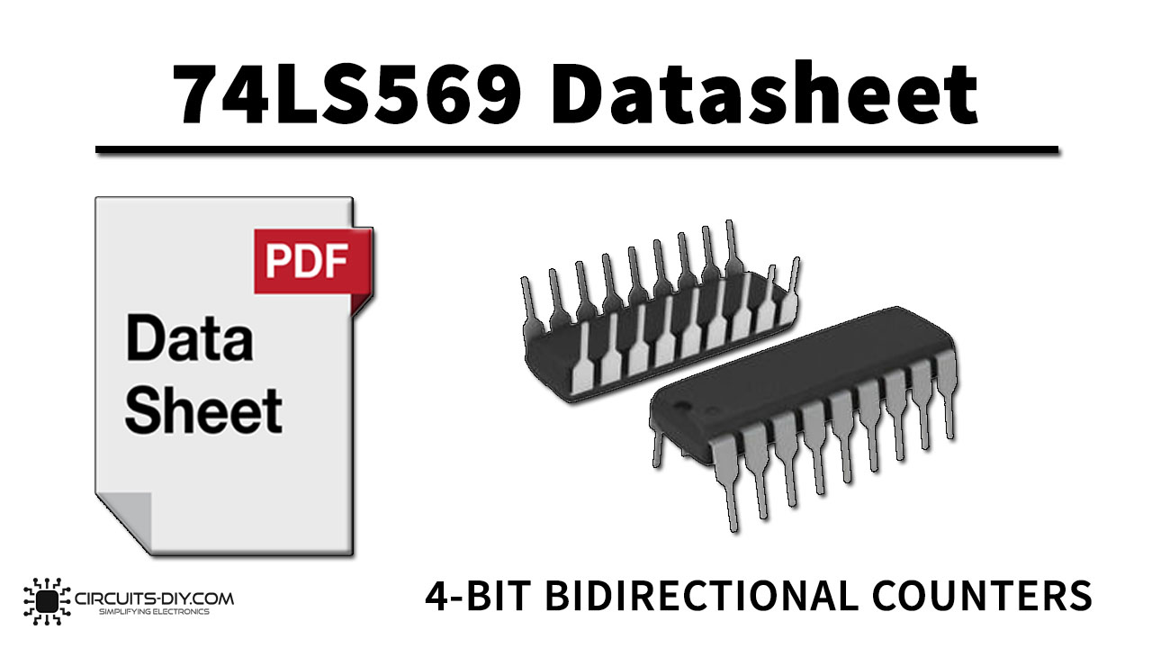
The 74F569/74LS569 is a fully synchronous Up/Down binary counter. It features preset capabilities for programmable operation, carry look ahead for programmable operation, carry look ahead for easy cascading, and U/D input to control the direction of counting. For maximum flexibility. It also features both Synchronous and Master Reset inputs as well as both Clocked Carry (CC) and Terminal Count (TC) outputs. All state changes except Master Reset are initiated by rising (+ve) edge of the clock. A High signal on the Output Enable (OE) input forces the output buffers into the high impedance state but does not prevent counting, resetting, or parallel loading. The output of the IC always comes in TTL which makes it easy to work with other TTL devices and microcontrollers. The IC 74F569 is compact in size and it has a much faster speed which makes it reliable in every kind of application.

What Binary Counter?
A Binary Counter is a serial digital counter that counts ten digits. it resets for every new clock input. As it can go through 10 unique combinations of output, it is also called as “Decade counter”. A binary counter can count 0000, 0001, 0010, 1000, 1001, 1010, 1011, 1110, 1111, 0000, and 0001 and so on. A 4 bit binary counter will act as a decade counter by skipping any six outputs out of the 16 (24) outputs.
74F569/74LS569 Key Features & Specifications
- Function: Counter
- Product type: Binary
- Rating: Catalog
- Package: DIP
- Pins: 16
- Bits: 4
- Operating Voltage: 5V
- Maximum clock frequency: 32MHz
- Synchronous counting
- Synchronously programmable
- Typical Rise Time: 18ns
- Typical Fall Time: 18ns
- Diode-clamped inputs
- Synchronous counting and loading
- Look ahead carry capability for easy cascading
- Preset capability for programmable operation
- Master Reset (MR) overrides all other inputs
- Synchronous Reset (SR) overrides counting and parallel loading
- Clock Carry (CC) output to be used as a clock for flip-flops, register, and counters
- 3-State outputs for bus organized systems
- 20 Pin DIP package
74F569/74LS569 Pinout
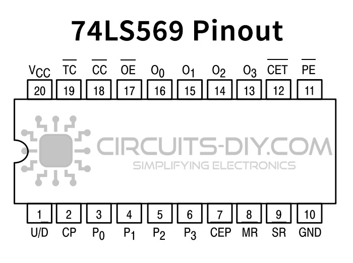
| Pin No. | Pin Name | Description |
|---|---|---|
| 1 | U/D’ | Up/Down count control input |
| 2 | CP | Clock Pulse Input |
| 3 | P0 | Parallel Data Input Pin P0 |
| 4 | P1 | Parallel Data Input Pin P1 |
| 5 | P2 | Parallel Data Input Pin P2 |
| 6 | P3 | Parallel Data Input Pin P3 |
| 7 | CEP’ | Active Low Count Enable Parallel Input Pin |
| 8 | MR’ | Active Low Master reset Input |
| 9 | SR’ | Active Low Synchronous Reset Input |
| 10 | GND | Ground Pin |
| 11 | PE’ | Active Low Parallel Enable Input |
| 12 | CET’ | Active Low Count Enable Trickle Input |
| 13 | O3 | Data Output O3 |
| 14 | O2 | Data Output O2 |
| 15 | O1 | Data Output O1 |
| 16 | O0 | Data Output O0 |
| 17 | OE’ | Active Low Output Enable |
| 18 | CC’ | Active Low Clocked Carry Output |
| 19 | TC’ | Active Low Terminal Count Output |
| 20 | Vcc | Chip Supply Voltage |
Applications
The 74F569/74LS569 IC has a number of different applications. A few of them are mentioned below:
- Astable frequency divider or counter circuit.
- Functions as a clock input for flip-flops, register, and counters.
74F569/74LS569 Datasheet
You can download the datasheet for 74F569/74LS569 4-Bit Bi-directional Counter IC With 3-State Output from the link given below:
See Also: 74LS10 Triple 3-Input NAND IC | 7404 NOT Gate IC | 74LS56 50-to-1 Frequency Divider IC

