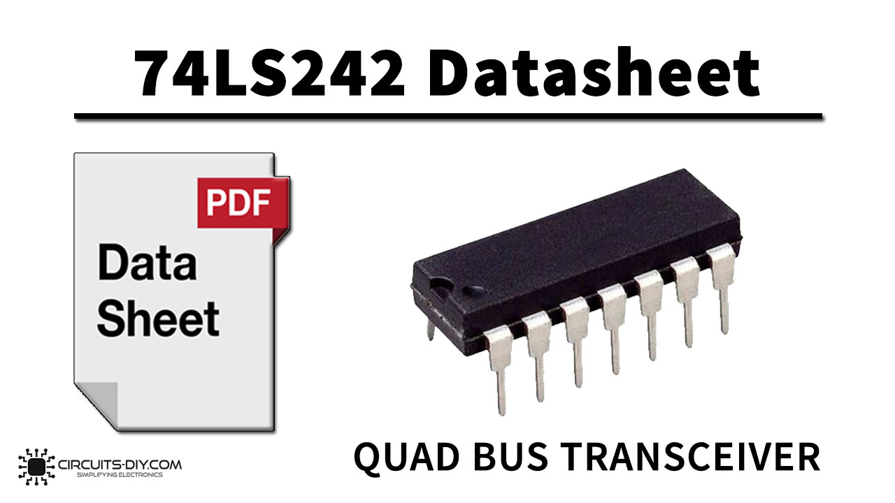
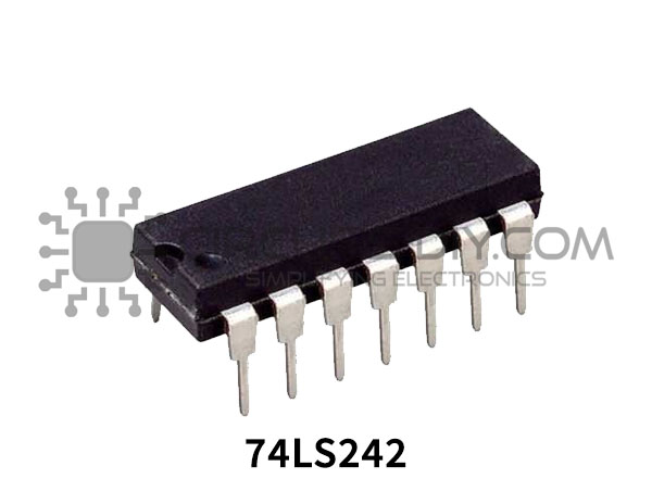
The 74LS242 IC is a Quad Bus Transmitter /Receiver designed for 4-line asynchronous 2-way data communications between data buses. The control function implementation minimizes external timing requirements. The 74LS242 IC has a vast array of working voltage, a wide range of working conditions, and directly interfaces with CMOS, NMOS, and TTL. The output of the IC always comes in TTL which makes it easy to work with other TTL devices and microcontrollers. The IC 74LS242 is smaller in size and it has a much faster speed which makes it reliable in every kind of device.
What is a Bus Transceiver?
Bus transceivers are electronic tri-state bi-directional devices that allow the flow of data between two points making them compatible with bus-oriented systems or the bi-directional (input or output) control of interface circuitry. A Bus transceiver can be inverting or non-inverting, common examples are 74LS243 & LS242 IC series. Bus transceivers are designed for asynchronous two-way communication between two data buses or input/output devices. The transceiver allows for the transmission of data from the terminals A to terminals B or the reverse depending on the logic level at the direction-control input.
74LS242 Key Features & Specifications
- Technology Family: LS
- VCC (Min): 4.75V
- VCC (Max): 5.25V
- Bits (#): 8
- Voltage at nominal operation: 5V
- Frequency at normal voltage (Max): 35MHz
- ICC at normal voltage (Max): 0.09mA
- Propagation delay (Max): 8ns – 12ns
- Input Clamp Diodes Limit High-Speed Termination Effects
- PNP Inputs Reduce DC Loading on Bus Lines
- Hysteresis at Bus Inputs Improves Noise Margins
- IOL (Max): 24mA
- IOH (Max): -15mA Rating: Catalog
- Operating temperature range: 0°C to 70°C
74LS242 Pinout
| Pin No. | Pin Name | Description |
|---|---|---|
| 1 | GBA’ | Active Low Enable Pin |
| 2 | NC | Not Used |
| 3 | 1A | Data Bus Input Pin 1A |
| 4 | 2A | Data Bus Input Pin 2A |
| 5 | 3A | Data Bus Input Pin 3A |
| 6 | 4A | Data Bus Input Pin 4A |
| 7 | GND | Ground Pin |
| 8 | 4B | Data Bus Input Pin 4B |
| 9 | 3B | Data Bus Input Pin 3B |
| 10 | 2B | Data Bus Input Pin 2B |
| 11 | 1B | Data Bus Input Pin 1B |
| 12 | NC | Not used |
| 13 | GBA | Active High Enable pin |
| 14 | Vcc | Chip Supply Voltage |

Applications
The 74LS242 Bus Transceiver has number of different applications, some of them are mentioned down below:
- Building Automation
- Electronic Point of Sale
74LS242 Datasheet
You can download the datasheet for 74LS242 Quadruple Bus Transceiver IC from the link provided below:
See Also: 74LS138 1-To-8 Decoder/Demultiplexer IC – Datasheet | 74LS45 BCD to Decimal Decoders/Drivers IC – Datasheet | 74LS31 Hex Delay Element/Delay Line Generator IC – Datasheet

