
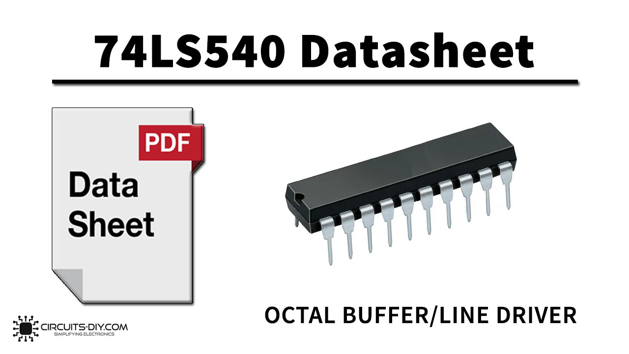
The 74LS540 IC is a part of the 74XXYY IC series. 74LS540 is 8-bit octal buffers and line drivers with the same functions as the LS240 and LS241 ICs. The IC is designed to be used as memory address drivers, clock drivers, and bus-oriented transmitters/receivers. These devices are especially useful as output ports for the microprocessors, allowing ease of layout and greater PC board density. 74LS540 IC has a wide range of working voltage, a wide range of working conditions, and directly interfaces with CMOS, NMOS, and TTL. The IC 74LS540 is smaller in size and it has a much faster speed which makes it reliable in every kind of device & other high speed, low noise applications.

Buffers & Line Drivers?
A buffer is a basic logic gate that passes its input, unchanged, to its output. Its behavior is the opposite of a NOT gate. The main purpose of a buffer is to regenerate the input, usually using a strong high and a strong low. A buffer has one input and one output; its output is always equal to its input. Buffers are also used to increase the propagation delay of circuits by driving the large capacitive loads.
On the other hand, Line drivers are a special type of buffer that includes the ability to drive a transmission line or cable that may be quite long. They also may adapt the input logic format to the specific line driving standard. An example of this is an eSATA Redriver.
74LS540 Pinout

74LS540 Pin Configuration
| Pin No | Pin Name | Description |
|---|---|---|
| 1 | OE0′ | Active Low 3-State Output Enable Input OE0′ |
| 2 | I0 | Data Input Pin I0 |
| 3 | I1 | Data Input Pin I1 |
| 4 | I2 | Data Input Pin I2 |
| 5 | I3 | Data Input Pin I3 |
| 6 | I4 | Data Input Pin I4 |
| 7 | I5 | Data Input Pin I5 |
| 8 | I6 | Data Input Pin I6 |
| 9 | I7 | Data Input Pin I7 |
| 10 | GND | Ground Pin |
| 11 | Y7′ | Complementary Data Output Pin Y7′ |
| 12 | Y6′ | Complementary Data Output Pin Y6′ |
| 13 | Y5′ | Complementary Data Output Pin Y5′ |
| 14 | Y4′ | Complementary Data Output Pin Y4′ |
| 15 | Y3′ | Complementary Data Output Pin Y3′ |
| 16 | Y2′ | Complementary Data Output Pin Y2′ |
| 17 | Y1′ | Complementary Data Output Pin Y1′ |
| 18 | Y0′ | Complementary Data Output Pin Y0′ |
| 19 | OE1′ | Active Low 3-State Output Enable Input OE1′ |
| 20 | Vcc | Chip Supply Voltage |
74LS540 Features & Specifications
- Technology Family: LS
- VCC (Min) (V): 4.75
- VCC (Max) (V): 5.25
- Channels (#): 8
- IOL (Max) (mA): 24
- ICC (Max) (uA): 52000
- IOH (Max) (mA): -15
- Input type: Bipolar
- Output type: 3-State
- Propagation speed: (tpd 10-50ns)
- Hysteresis at Inputs to Improve Noise Margin
- PNP Inputs Reduce Loading
- 3-State Outputs Drive Bus Lines
- Inputs and Outputs Opposite Side of Package
- Input Clamp Diodes Limit High-Speed Termination Effects
- Data rate (Mbps): 70
- Rating Catalog
Applications
- Generally used to isolate other gates or circuit stages from each other preventing the impedance of one circuit from affecting the impedance of another circuit.
You can download this datasheet for 74LS540 Octal Buffers and Line Drivers with 3-State Outputs from the link given below:
See Also: 74LS153 Dual 4 To 1 Line Multiplexer IC – Datasheet | 74LS135 Quad 2-Input XOR Logic Gate IC – Datasheet | 74LS135 Quad 2-Input XOR Logic Gate IC – Datasheet


1 thought on “74LS540 Octal Buffers and Line Drivers with 3-State Outputs | Datasheet”
Comments are closed.