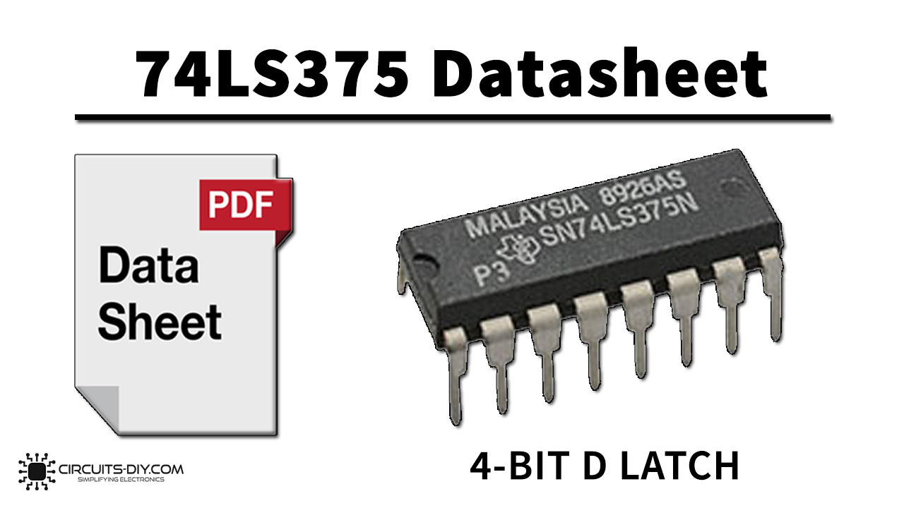
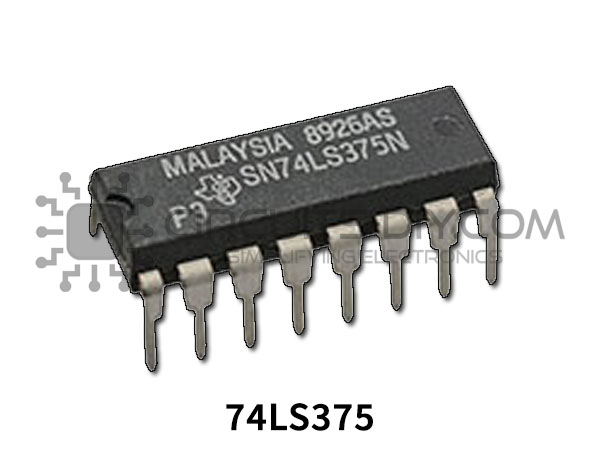
The 74LS375 IC is a part of the 74XXYY IC series. The 74LS375 IC is a 4-Bit D-Type Latch for use as temporary storage for binary information between processing limits and input /output or indicator units. When the Enable (E) is HIGH, information present at the D input will be transferred to the Q output and, if E is HIGH, the Q output will follow the input. When E goes LOW, the information present at the D input prior to its setup time will be retained at the Q outputs. 74LS375 IC has a wide range of working voltage, a wide range of working conditions, and directly interfaces with CMOS, NMOS, and TTL. The IC 74LS375 is smaller in size and it has a much faster speed which makes it reliable in every kind of device.
What is a D-Type Latch/Flip-Flop?
A D-type Latch/flip-flop is best described as a clocked latch, that has two stable states. A D-type latch operates with a delay in input by one clock cycle. Thus, by cascading many D-type flip-flops delay circuits can be created, which are used in many applications such as in digital television systems. A D-type flip-flop is also known as a D flip-flop or a delay flip-flop.
74LS375 Pinout
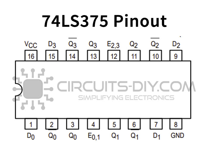
74LS375 Pin Configuration
| Pin No | Pin Name | Description |
|---|---|---|
| 1 | D0 | Data Input Pin 0 |
| 2 | Q0′ | Complementary Latch output pin Q0′ |
| 3 | Q0 | Latch output pin Q0 |
| 4 | E(0,1) | Enable Input Latches 0, 1 |
| 5 | Q1 | Latch output pin Q1 |
| 6 | Q1′ | Complementary Latch output pin Q1′ |
| 7 | D1 | Data Input Pin 1 |
| 8 | GND | Ground Pin |
| 9 | D2 | Data Input Pin 2 |
| 10 | Q2′ | Complementary Latch output pin Q2′ |
| 11 | Q2 | Latch output pin Q2 |
| 12 | E(2,3) | Enable Input Latches 2, 3 |
| 13 | Q3 | Latch output pin Q3 |
| 14 | Q3′ | Complementary Latch output pin Q3′ |
| 15 | D3 | Data Input Pin 3 |
| 16 | Vcc | Chip Supply Voltage |
74LS375 Features & Specifications
- Function: D-Type latch
- Channels (#): 4
- Technology Family: LS
- VCC (Min): 4.75V
- VCC (Max): 5.25V
- Input type: Bipolar
- Output type: Push-Pull
- Data rate (Max): 70Mbps
- IOL (Max): 8mA
- IOH (Max): -0.4mA
- Propagation speed: (TPD 5-10ns)
- Ideal for Temporary Storage Applications
- Inputs are Diode Clamped
- Operating Temperature up to 70°C
- Standard TTL Switching Voltages
Applications
- Best suited for use as temporary storage unit for binary information between processing units & I/O or indicator units.
You can download this datasheet for 74LS375 datasheet from the link given below:
See Also: 74LS164 8-Bit Shift Register IC With Parallel Outputs – Datasheet | 74LS157 Quad 2 To 1 Line Multiplexer IC – Datasheet | 74LS132 Quad 2-Input Schmitt trigger NAND Gate IC – Datasheet


