The 74LS299 is an 8-Bit Universal Shift/Storage Register with 3-state outputs. Four modes of operation are possible: hold (store), shift left, shift right, and load data. The 74LS399 IC has a wide range of working voltage, a wide range of working conditions, offers a wide variety of features such as ESD protection & thermal overload protection and directly interfaces with CMOS, NMOS, and TTL. The output of the IC always comes in TTL which makes it easy to work with other TTL devices and microcontrollers.

What is a Storage/Shift Register?
Storage/Shift registers are digital memory circuitry found in devices such as calculators, computers, and data processing systems. With a shift register, data or bits are entered into the system in a serial or parallel manner. data entry is done from one direction, and as more data is added, it shifts positions until the data gets to the output end. The two ends are referred to as the left and right end. The movement of data can be from left to right, from right to left, or in both directions to make a bidirectional register.
74LS299 Pinout
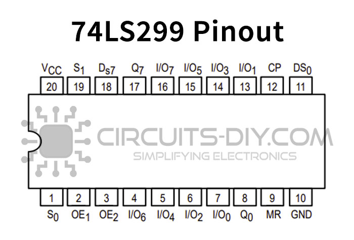
74LS299 Pin Configuration
| Pin No | Pin Name | Description |
|---|---|---|
| 1 | S0 | Mode Select Input Pin |
| 2 | OE1‘ | Active Low 3-State Output Enable Pin 1 |
| 3 | OE2‘ | Active Low 3-State Output Enable Pin 2 |
| 4 | I/O6 | Parallel Data Input Pin I/O6 |
| 5 | I/O4 | Parallel Data Input Pin I/O4 |
| 6 | I/O2 | Parallel Data Input Pin I/O2 |
| 7 | I/O0 | Parallel Data Input Pin I/O0 |
| 8 | Q0 | Serial Output Pin |
| 9 | MR’ | Active Low Asynchronous Master Reset Input |
| 10 | GND | Ground Pin |
| 11 | DS0 | Serial Data Input pin for Right Shift |
| 12 | CP | Clock Pulse Input |
| 13 | I/O1 | Parallel Data Input Pin I/O1 |
| 14 | I/O3 | Parallel Data Input Pin I/O3 |
| 15 | I/O5 | Parallel Data Input Pin I/O5 |
| 16 | I/O7 | Parallel Data Input Pin I/O7 |
| 17 | Q7 | Serial Output Pin |
| 18 | DS7 | Serial Data Input pin for Left Shift |
| 19 | S1 | Mode Select Input Pin |
| 20 | Vcc | Chip Supply Voltage |
74LS299 Features & Specifications
- Bits (#): 8
- Technology Family: LS
- VCC (Min) (V): 4.75
- VCC (Max) (V): 5.25
- Input type: TTL
- Output type: TTL
- IOL (Max) (mA): 24
- IOH (Max) (mA): -2.6
- Multiplexed Input/Outputs for Data Hold, Shift Right, Shift Left, and Load Data
- Operates with Outputs Enabled or at High impedance
- Common I/O for Reduced Pin Count
- Four Operation Modes: Shift Left, Shift Right, Load and Store
- Separate Shift Right Serial Input and Shift Left Serial Input for Easy Cascading
- 3-State Outputs Drive Bus Lines Directly
- Can be Cascaded for N-Bit Word Lengths
- Standard TTL Switching Voltages
Applications
- Sequence generation circuits
- Memory Defragmentation Circuits used in system repair
You can download this datasheet for 74LS299 Storage/Shift Register IC With 3-State Outputs from the link given below:
See Also: 74LS157 Quad 2 To 1 Line Multiplexer IC – Datasheet | 74LS139 Dual 1-Of-4 Decoder/Demultiplexer IC – Datasheet | 74LS132 Quad 2-Input Schmitt trigger NAND Gate IC – Datasheet