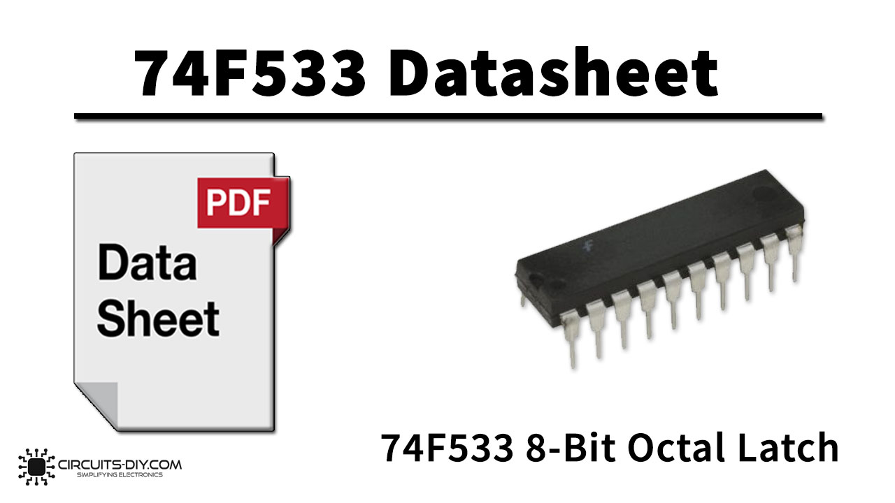
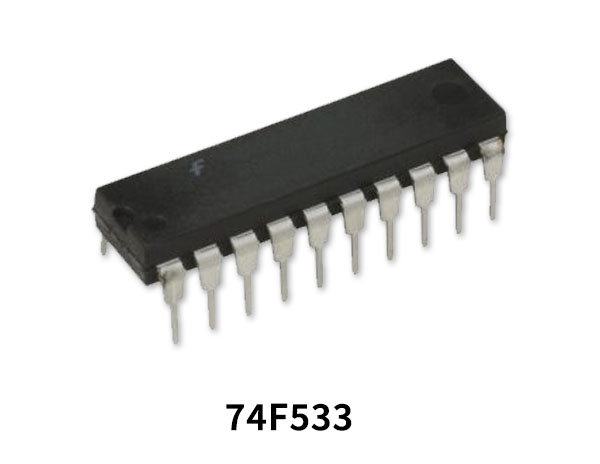
74F533 IC consists of eight latches with 3-state outputs for bus organized system applications. The flip-flops appear transparent to the data when Latch Enable (LE) is HIGH. When LE is LOW, the data that meets the setup times is latched. The 3-State buffers are controlled by the Output Enable (OE’) input. When OE’ is LOW, the buffers are in the bi-state mode. When OE’ is HIGH the buffers are in the high impedance mode, but this does not interfere with entering new data into the latches. 74F533 IC has a wide range of working voltage, a wide range of working conditions, and directly interfaces with CMOS, NMOS, and TTL. The IC 74F533 is smaller in size and it has a much faster speed which makes it reliable in every kind of device.
What is a Latch Circuit?
A latch is a device that can be used to store one bit of information. A latching circuit is used to capture, or ‘latch’ the logic level which is present on the Data line when the clock input is high. If the data on the Data line changes state while the clock pulse is high, then the output, Q, follows the input, D. When the CLK input falls to logic 0, the last state of the Data input is trapped and held in the latch.
74F533 Pinout
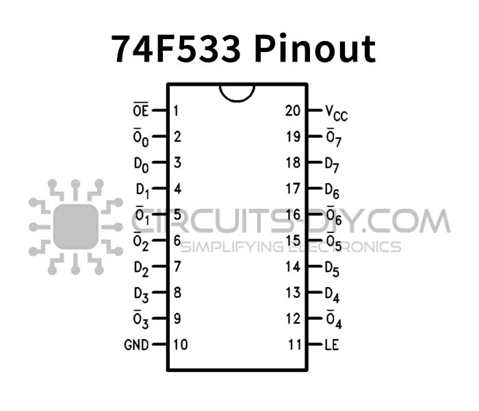
74F533 Pin Description
| Pin No. | Pin Name | Description |
|---|---|---|
| 1 | OE’ | Active Low Output Enable Pin |
| 2 | O0′ | Complementary Tri-State Output O0′ |
| 3 | D0 | Data Input Pin D0 |
| 4 | D1 | Data Input Pin D1 |
| 5 | O1′ | Complementary Tri-State Output O1′ |
| 6 | O2′ | Complementary Tri-State Output O2′ |
| 7 | D2 | Data Input Pin D2 |
| 8 | D3 | Data Input Pin D3 |
| 9 | O3′ | Complementary Tri-State Output O3′ |
| 10 | GND | Ground Pin |
| 11 | LE | Latch Enable Input |
| 12 | O4′ | Complementary Tri-State Output O4′ |
| 13 | D4 | Data Input Pin D4 |
| 14 | D5 | Data Input Pin D5 |
| 15 | O5′ | Complementary Tri-State Output O5′ |
| 16 | O6′ | Complementary Tri-State Output O6′ |
| 17 | D6 | Data Input Pin D6 |
| 18 | D7 | Data Input Pin D7 |
| 19 | O7′ | Complementary Tri-State Output O7′ |
| 20 | Vcc | Chip Supply Voltage |
74F533 Key Features & Specifications
- Function: Octal latch
- Channels (#): 8
- Technology Family: F
- VCC (Min): 4.75V
- VCC (Max): 5.25V
- Input type: Bipolar
- Output type: Push-Pull
- IOL (Max): 8mA
- IOH (Max): -0.4mA
- Propagation speed: (TPD 5-10ns)
Applications
- Usually used as a storage device in power gating circuits and clocks.
- Also used as an input/output port in asynchronous systems.
You can download this datasheet for 74F533 Octal Transparent Latch IC with Tri-State Outputs from the link given below:
See Also: 74LS157 Quad 2 To 1 Line Multiplexer IC – Datasheet | 74LS150 16-1 Data Selector Multiplexer IC – Datasheet | 74LS83 4-Bit Binary Full Adder IC With Fast Carry | Datasheet


