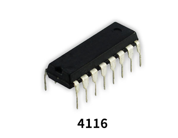
The 4116 is a new generation MOS dynamic random access memory circuit organized as 16,384 words by, 1 bit. As a state-of-the-art MOS memory device, the 4116 (16K advanced circuit techniques are designed to provide wide operating margins, both internally and to the system in speed and power previously seen only in MOSTEK’s high-performance MK 4027 (4K RAM).
This process, coupled with the use of a single transistor dynamic storage cell, provides the maximum possible circuit density and reliability while maintaining high-performance double-poly, N-channel silicon gate capability. out, including sense amplifiers, assures that power The use of dynamic circuitry through dissipation is minimized without any sacrifice in speed or operating margin. These factors combine to make the 4116 a truly superior

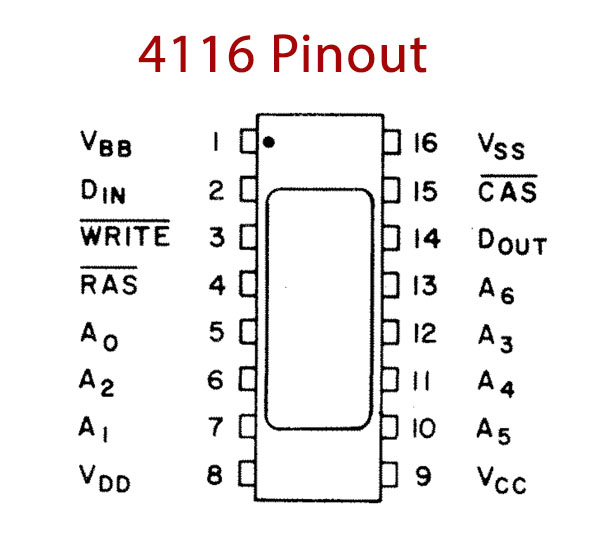
4116 Pinout

4116 Pin Configuration
| Pin No | Pin Name | Description |
|---|---|---|
| 1 | VBB | Supply Voltage |
| 2 | DIN | Data In |
| 3 | WRITE’ | Read/Write Input |
| 4 | RAS’ | Row Address Strobe |
| 5 | A0 | Address Pin 0 |
| 6 | A2 | Address Pin 2 |
| 7 | A1 | Address Pin 1 |
| 8 | VDD | Supply Voltage |
| 9 | VCC | Power Voltage |
| 10 | A5 | Address Pin 5 |
| 11 | A4 | Address Pin 4 |
| 12 | A3 | Address Pin 3 |
| 13 | A6 | Address Pin 6 |
| 14 | D OUT | Data Out |
| 15 | CAS’ | Column Address Strobe |
| 16 | VSS | Ground Pin |
4116 Key Feature
- Recognized industry standard 16-pin configuration from MOSTEK
- 150ns access time, 320ns cycle (MK 4116-2) 200ns access time, 375ns cycle (MK 4116-3)
- 10% tolerance on all power supplies (+12V, +5V)
- Low power: 462mW active, 20mW standby (max)
- Output data controlled by CAS and unlatched at end of cycle to allow two dimensional chip selection and extended page boundary
You can download this datasheet for 4116 16k Video RAM – Datasheet from the link given below:


