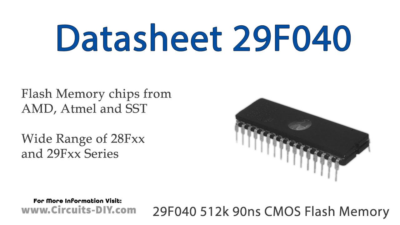
The 29F040B is a 4 Mbit, 5.0 volt-only Flash memory organized as 524,288 Kbytes of 8 bits each. The 512 Kbytes of data are divided into eight sectors of 64 Kbytes each for flexible erase capability. The 8 bits of data appear on DQ0–DQ7. The 29F040B is offered in 32-pin PLCC, TSOP, and PDIP packages. This device is designed to be programmed in-system with the standard system 5.0 volt VCC supply. A 12.0-volt VPP is not required for write or erase operations. The device can also be programmed by standard EPROM programmers.
This device is manufactured using AMD’s 0.35 µm process technology and offers all the features and benefits of the 29F040, which was manufactured using 0.5 µm process technology. In addition, the Am29F040B has a second toggle bit, DQ2, and also offers the ability to program in the Erase Suspend mode.
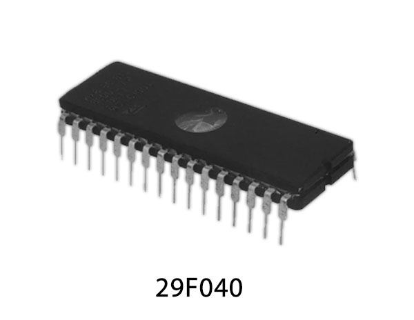
29F040 Pinout
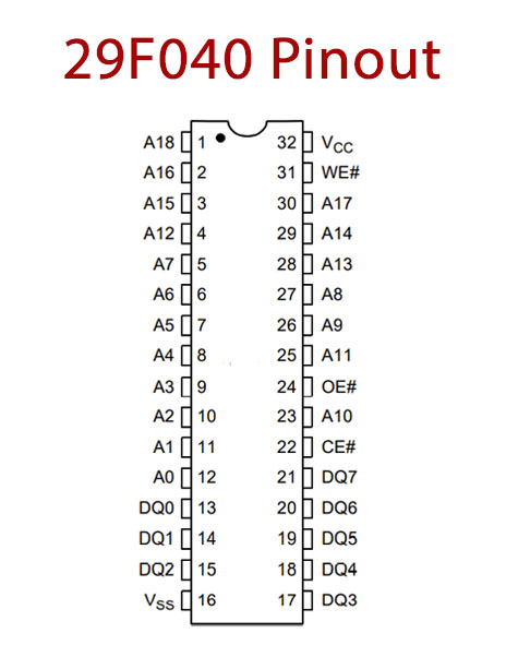
29F040 Pin Configuration
| Pin No | Pin Name | Description |
|---|---|---|
| 1 | A18 | Address Pin 18 |
| 2 | A16 | Address Pin 16 |
| 3 | A15 | Address Pin 15 |
| 4 | A12 | Address Pin 12 |
| 5 | A7 | Address Pin 7 |
| 6 | A6 | Address Pin 6 |
| 7 | A5 | Address Pin 5 |
| 8 | A4 | Address Pin 4 |
| 9 | A3 | Address Pin 3 |
| 10 | A2 | Address Pin 2 |
| 11 | A1 | Address Pin 1 |
| 12 | A0 | Address Pin 0 |
| 13 | DQ 0 | Data Output 0 |
| 14 | DQ 1 | Data Output 1 |
| 15 | DQ 2 | Data Output 2 |
| 16 | VSS | Ground Pin |
| 17 | DQ 3 | Data Output 3 |
| 18 | DQ 4 | Data Output 4 |
| 19 | DQ 5 | Data Output 5 |
| 20 | DQ 6 | Data Output 6 |
| 21 | DQ 7 | Data Output 7 |
| 22 | CE’ | Chip Enable Pin |
| 23 | A10 | Address Pin 10 |
| 24 | OE’ | Output Enable Pin |
| 25 | A11 | Address Pin 11 |
| 26 | A9 | Address Pin 9 |
| 27 | A8 | Address Pin 8 |
| 28 | A13 | Address Pin 13 |
| 29 | A14 | Address Pin 14 |
| 30 | A17 | Address Pin 17 |
| 31 | WE’ | Write Enable Pin |
| 32 | VCC | Power Supply |
29F040 Key Feature
- 5.0 V ± 10% for read and write operations
- Minimizes system level power requirements
- Manufactured on 0.35 µm process technology
- Compatible with 0.5 µm Am29F040 device
- High performance
- Access times as fast as 55 ns
- Low power consumption
- 20 mA typical active read current
- 30 mA typical program/erase current time to active mode)
- Flexible sector architecture
- 8 uniform sectors of 64 Kbytes each
- Any combination of sectors can be erased
- Supports full chip erase
You can download this datasheet for 29F040 512k 90ns CMOS Flash Memory – Datasheet from the link given below:

