The 29F020B Family consists of 2 Mbit, 5.0 volt-only Flash memory devices organized as 262,144 bytes. The 29F020B offers the RESET# function, the 29F020B does not. The data appears on DQ7–DQ0. The device is offered in 32-pin PLCC, 32-pin TSOP, and 32-pin PDIP packages. This device is designed to be programmed in-system with the standard system 5.0 volt VCC supply. No VPP is required for write or erases operations.
The device can also be programmed by standard EPROM programmers. This device is manufactured using AMD’s 0.32 µm process technology and offers all the features and benefits of the 29F020, which was manufactured using 0.5 µm process technology. The standard device offers access times of 55, 70, 90, and 120 ns, allowing high-speed microprocessors to operate without wait states. To eliminate bus contention the device has a separate chip enable (CE#), write enable (WE#) and output-enable (OE#) controls

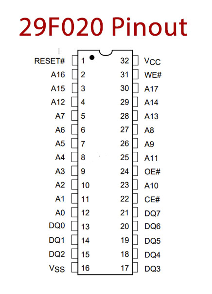
29F020 Pinout

29F020 Pin Configuration
| Pin No | Pin Name | Description |
|---|---|---|
| 1 | RESET | Reset Pin |
| 2 | A16 | Address Pin 16 |
| 3 | A15 | Address Pin 15 |
| 4 | A12 | Address Pin 12 |
| 5 | A7 | Address Pin 7 |
| 6 | A6 | Address Pin 6 |
| 7 | A5 | Address Pin 5 |
| 8 | A4 | Address Pin 4 |
| 9 | A3 | Address Pin 3 |
| 10 | A2 | Address Pin 2 |
| 11 | A1 | Address Pin 1 |
| 12 | A0 | Address Pin 0 |
| 13 | DQ 0 | Data Output 0 |
| 14 | DQ 1 | Data Output 1 |
| 15 | DQ 2 | Data Output 2 |
| 16 | Vss | Ground Pin |
| 17 | DQ 3 | Data Output 3 |
| 18 | DQ 4 | Data Output 4 |
| 19 | DQ 5 | Data Output 5 |
| 20 | DQ 6 | Data Output 6 |
| 21 | DQ 7 | Data Output 7 |
| 22 | CE’ | Chip Enable Pin |
| 23 | A10 | Address Pin 10 |
| 24 | OE’ | Output Enable Pin |
| 25 | A11 | Address Pin 11 |
| 26 | A9 | Address Pin 9 |
| 27 | A8 | Address Pin 8 |
| 28 | A13 | Address Pin 13 |
| 29 | A14 | Address Pin 14 |
| 30 | A17 | Address Pin 17 |
| 31 | WE’ | Write Enable Pin |
| 32 | VCC | Power Supply |
29F020 Key Feature
- Single power supply operation
- 5.0 Volt-only operation for read, erase, and
- program operations
- Minimizes system-level requirements
- Manufactured on 0.32 µm process technology
- Compatible with 0.5 µm Am29F002 device
- High performance
- Access times as fast as 55 ns
- Low power consumption (typical values at 5 MHz)
- 1 µA standby mode current
- 20 mA read current
- 30 mA program/erase current
- Flexible sector architecture
- One 16 Kbyte, two 8 Kbyte, one 32 Kbyte, and three 64 Kbyte sectors
- Supports full chip erase
You can download this datasheet for 29F020 256k 120ns CMOS Flash Memory – Datasheet from the link given below:


