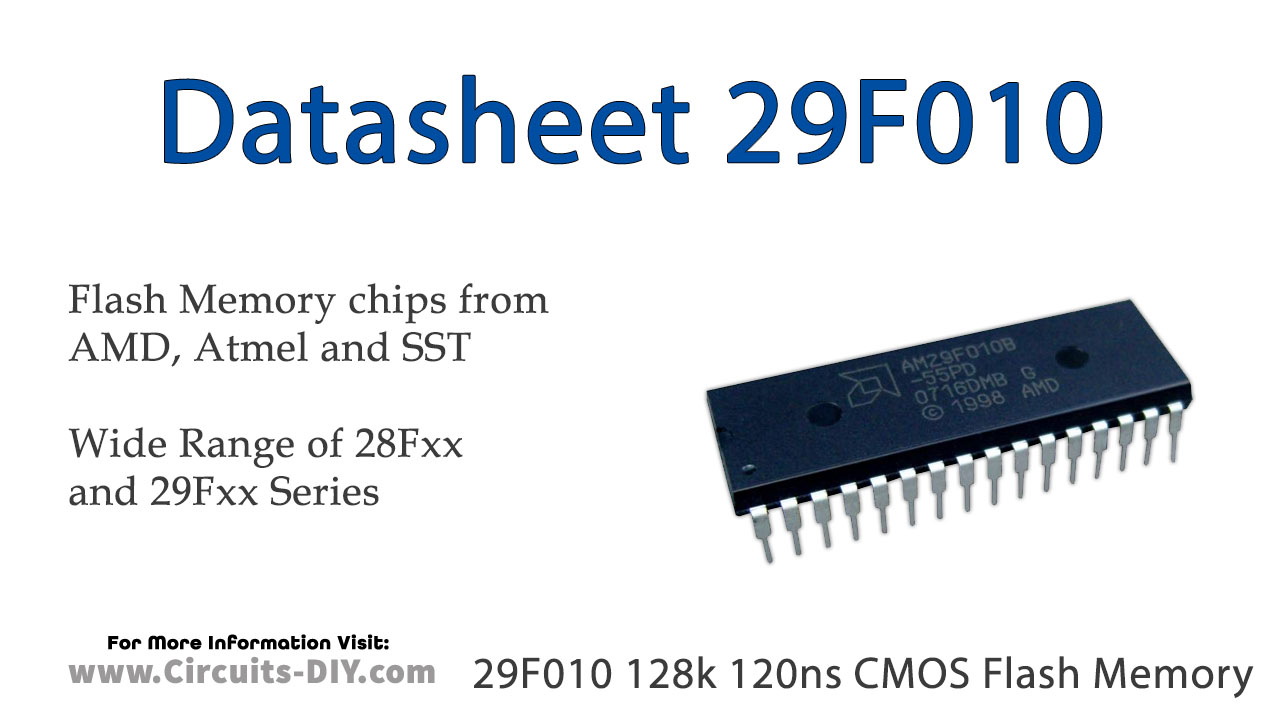
The Am29F010 is a 1 Mbit, 5.0 Volt-only Flash memory organized as 131,072 bytes. The Am29F010 is offered in 32-pin PLCC, TSOP, and PDIP packages. The byte data appears on DQ0-DQ7. The device is designed to be programmed in-system with the standard system 5.0 Volt VCC supply. A 12.0-volt VPP is not required for program or erase operations. The device can also, be programmed or erased by standard EPROM programmers.
The standard device offers access times of 45, 55, 70, 90, and 120 ns, allowing high-speed microprocessors to operate without wait states. To eliminate bus contention the device has a separate chip enable (CE#), write enable (WE#) and output-enable (OE) controls. The device requires only a single 5.0-volt power supply for both read and write functions. Internally generated and regulated voltages are provided for the program and erase operations
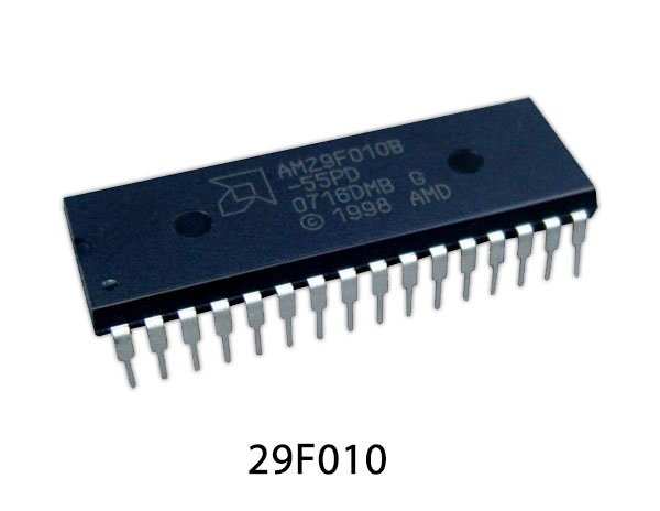
29F010 Pinout
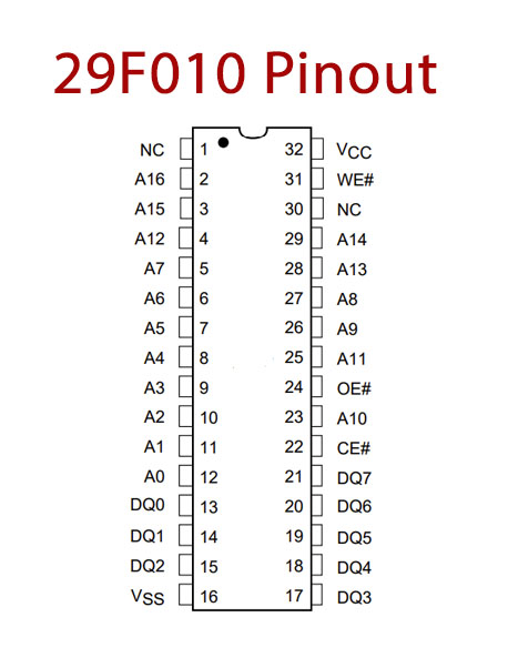
29F010 Pin Configuration
| Pin No | Pin Name | Description |
|---|---|---|
| 1 | NC | No Connection |
| 2 | A16 | Address Pin 16 |
| 3 | A15 | Address Pin 15 |
| 4 | A12 | Address Pin 12 |
| 5 | A7 | Address Pin 7 |
| 6 | A6 | Address Pin 6 |
| 7 | A5 | Address Pin 5 |
| 8 | A4 | Address Pin 4 |
| 9 | A3 | Address Pin 3 |
| 10 | A2 | Address Pin 2 |
| 11 | A1 | Address Pin 1 |
| 12 | A0 | Address Pin 0 |
| 13 | DQ 0 | Data Output 0 |
| 14 | DQ 1 | Data Output 1 |
| 15 | DQ 2 | Data Output 2 |
| 16 | VSS | Ground Pin |
| 17 | DQ 3 | Data Output 3 |
| 18 | DQ 4 | Data Output 4 |
| 19 | DQ 5 | Data Output 5 |
| 20 | DQ 6 | Data Output 6 |
| 21 | DQ 7 | Data Output 7 |
| 22 | CE’ | Chip Enable Pin |
| 23 | A10 | Address Pin 10 |
| 24 | OE’ | Output Enable Pin |
| 25 | A11 | Address Pin 11 |
| 26 | A9 | Address Pin 9 |
| 27 | A8 | Address Pin 8 |
| 28 | A13 | Address Pin 13 |
| 29 | A14 | Address Pin 14 |
| 30 | NC | No Connection |
| 31 | WE | Write Enable Pin |
| 32 | VCC | Power Supply |
29F010 Key Feature
- Single power supply operation
- 5.0 V ± 10% for read, erase, and program operations
- Simplifies system-level power requirements
- High performance
- 45 ns maximum access time
- Low power consumption
- 30 mA max active read current
- 50 mA max program/erase current
- <25 µA typical standby current
- Flexible sector architecture
- Eight uniform sectors
- Any combination of sectors can be erased
- Supports full chip erase
- Sector protection
- Hardware-based feature that disables/reenables program and erase operations in any combination of sectors
- Sector protection/unprotection can be implemented using standard PROM programming equipment
You can download this datasheet for 29F010 128k 120ns CMOS Flash Memory – Datasheet from the link given below:


