The 28F512 CMOS flash memory offers the most cost-effective and reliable alternative for reading/write random access nonvolatile memory. The 28F512 adds electrical chip-erasure and reprogramming to familiar EPROM technology. Memory contents can be rewritten: in a test socket; in a PROM-programmer socket; onboard during subassembly test; in-system during the final test; and in-system after-sale. The 28F512 increases memory flexibility while contributing to time- and cost savings.
The 28F512 is a 512-kilobit nonvolatile memory organized as 65,536 bytes of 8 bits. Intel’s 28F512 is offered in 32-pin plastic dip or 32-lead PLCC packages. Pin assignments conform to JEDEC standards for byte-wide EPROMs. Extended erase and program cycling capability is designed into Intel’s ETOX II (EPROM Tunnel Oxide) process technology. Advanced oxide processing, an optimized tunneling structure, and lower electric field combine to extend reliable cycling beyond that of traditional EEPROMs. With the 12.0V Vpp supply, the 28F512 performs 100,000 erase and program cycles well within the time limits of the Quick-Pulse Programming and Quick-Erase algorithms.
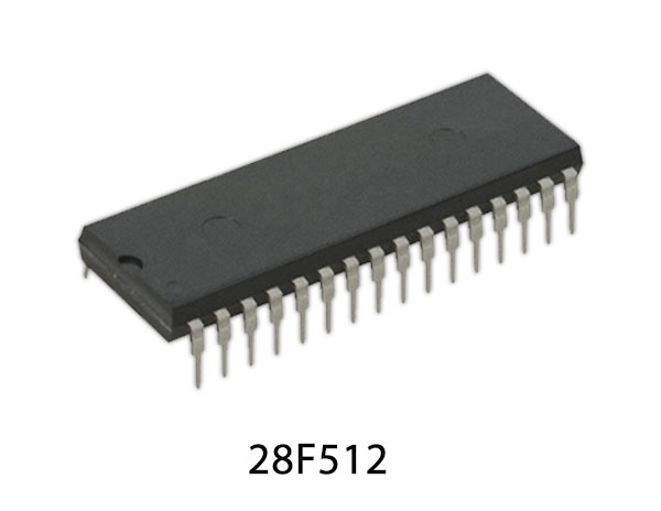
28F512 Pinout
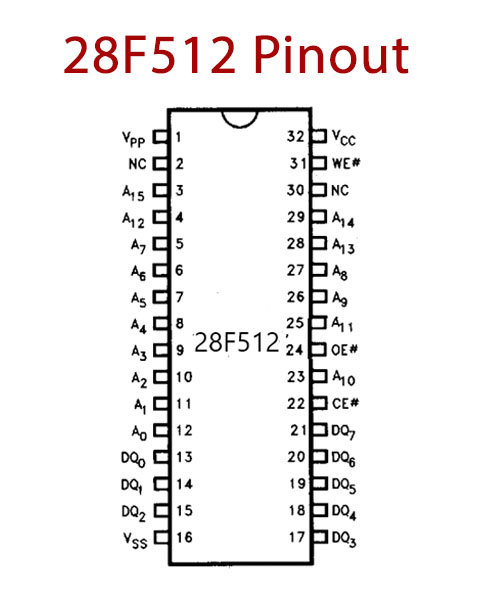
28F512 Pin Configuration
| Pin No | Pin Name | Description |
|---|---|---|
| 1 | VPP | Programming Supply |
| 2 | NC | No Connection |
| 3 | A15 | Address Pin 15 |
| 4 | A12 | Address Pin 12 |
| 5 | A7 | Address Pin 7 |
| 6 | A6 | Address Pin 6 |
| 7 | A5 | Address Pin 5 |
| 8 | A4 | Address Pin 4 |
| 9 | A3 | Address Pin 3 |
| 10 | A2 | Address Pin 2 |
| 11 | A1 | Address Pin 1 |
| 12 | A0 | Address Pin 0 |
| 13 | DQ 0 | Data Output 0 |
| 14 | DQ 1 | Data Output 1 |
| 15 | DQ 2 | Data Output 2 |
| 16 | VSS | Ground Pin |
| 17 | DQ 3 | Data Output 3 |
| 18 | DQ 4 | Data Output 4 |
| 19 | DQ 5 | Data Output 5 |
| 20 | DQ 6 | Data Output 6 |
| 21 | DQ 7 | Data Output 7 |
| 22 | CE’ | Chip Enable Pin |
| 23 | A10 | Address Pin 10 |
| 24 | OE’ | Output Enable Pin |
| 25 | A11 | Address Pin 11 |
| 26 | A9 | Address Pin 9 |
| 27 | A8 | Address Pin 8 |
| 28 | A13 | Address Pin 13 |
| 29 | A14 | Address Pin 14 |
| 30 | NC | No Connection |
| 31 | WE | Write Enable Pin |
| 32 | VCC | Power Supply |
28F512 Key Feature
- Flash Electrical Chip-Erase
- 1 Second Typicai Chip-Erase
- Quick-Pulse Programming Algorithm
- 10 s Typical Byte-Program
- 1 Second Chip-Program
- 100,000 Erase/Program Cycles
- 12.0V 5% Vpp
- High-Performance Read
- 120 ns Maximum Access Time
- CMOS Low Power Consumptlon
- 10 mA Typical Actlve Current
- 50 A Typical Standby Current
- 0W Data Retention Power
- Integrated Program/Erase Stop Timers
You can download this datasheet for 28F512 512k 150ns CMOS Flash Memory – Datasheet from the link given below:


