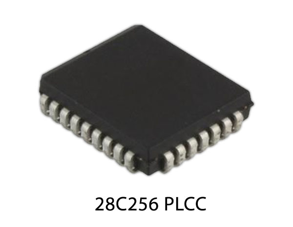
The AT28C256 is a high-performance electrically erasable and programmable read-only memory. Its 256K of memory is organized as 32,768 words by 8 bits. . When the device is deselected, the CMOS standby current is less than 200 µA. The AT28C256 is accessed like a Static RAM for the read or write cycle without the need for external components. The device contains a 64-byte page register to allow writing of up to 64 bytes simultaneously. During a write cycle, the addresses and 1 to 64 bytes of data are internally latched, freeing the address and data bus for other operations. Following the initiation of a write cycle, the device will automatically write the latched data using an internal control timer.
Once the end of a write cycle has been detected a new access for reading or write can begin.

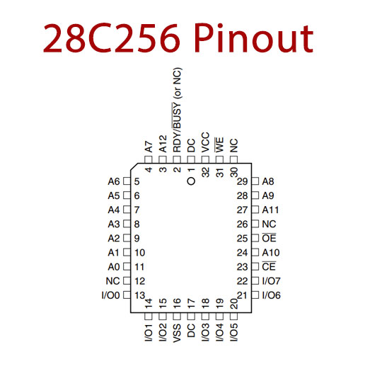
28C256 Pinout

28C256 Pin Configuration
| Pin No | Pin Name | Description |
| 1 | DC | Don’t Connect |
| 2 | BUSY’ | Busy Pin |
| 3 | A12 | Address Pin 12 |
| 4 | A7 | Address Pin 7 |
| 5 | A6 | Address Pin 6 |
| 6 | A5 | Address Pin 5 |
| 7 | A4 | Address Pin 4 |
| 8 | A3 | Address Pin 3 |
| 9 | A2 | Address Pin 2 |
| 10 | A1 | Address Pin 1 |
| 11 | A0 | Address Pin 0 |
| 12 | NC | No Connection |
| 13 | I/O 0 | Data Inputs/Outputs 0 |
| 14 | I/O 1 | Data Inputs/Outputs 1 |
| 15 | I/O 2 | Data Inputs/Outputs 2 |
| 16 | Vss | Ground Pin |
| 17 | DC | Don’t Connect |
| 18 | I/O 3 | Data Inputs/Outputs 3 |
| 19 | I/O 4 | Data Inputs/Outputs 4 |
| 20 | I/O 5 | Data Inputs/Outputs 5 |
| 21 | I/O 6 | Data Inputs/Outputs 6 |
| 22 | I/O 7 | Data Inputs/Outputs 7 |
| 23 | CE’ | Chip Enable Pin |
| 24 | A10 | Address Pin 10 |
| 25 | OE’ | Output Enable |
| 26 | NC | No Connection |
| 27 | A11 | Address Pin 11 |
| 28 | A9 | Address Pin 9 |
| 29 | A8 | Address Pin 8 |
| 30 | NC | No Connection |
| 31 | WE’ | Write Enable |
| 32 | VCC | Power Supply |
28C256 Key Feature
- Fast Read Access Time – 150 ns
- Automatic Page Write Operation
- Internal Address and Data Latches for 64 Bytes
- Internal Control Timer
- Fast Write Cycle Times
- Page Write Cycle Time: 3 ms or 10 ms Maximum
- 1 to 64-byte Page Write Operation
- Low Power Dissipation
- 50 mA Active Current
- 200 µA CMOS Standby Current
- Hardware and Software Data Protection
- DATA Polling for End of Write Detection
- High-Reliability CMOS Technology
- Endurance: 10^4 or 10^5 Cycles
- Data Retention: 10 Years
- Single 5V ± 10% Supply
- CMOS and TTL Compatible Inputs and Outputs
- JEDEC Approved Byte-wide Pinout
- Full Military, Commercial, and Industrial Temperature Ranges
- Green (Pb/Halide-free) Packaging Option
You can download this datasheet for 28C256 256K 250ns Parallel PLCC EEPROM – Datasheet from the link given below:


