This 25-bit 1:1 or 14-bit 1:2 configurable registered buffer is designed for 1.7-V to 1.9-V VDD operation. All clock and data inputs are compatible with the JEDEC standard for SSTL_18. The control inputs are LVCMOS. All outputs are 1.8-V CMOS drivers that have been optimized to drive the DDR-II DIMM load. ICSSSTUF32864A operates from a differential clock (CK and CK#). Data are registered at the crossing of CK going high, and CK# going low.
The C0 input controls the pinout configuration of the 1:2 pinout from A configuration (when low) to B configuration (when high). The C1 input controls the pinout configuration from 25-bit 1:1 (when low) to 14-bit 1:2 (when high). The device supports low-power standby operation. When the reset input (RST#) is low, the differential input receivers are disabled, and undriven (floating) data, clock, and reference voltage (VREF) inputs are allowed. In addition, when RST# is low all registers are reset, and all outputs are forced low. The LVCMOS RST# and Cn inputs must always be held at a valid logic high or low level.
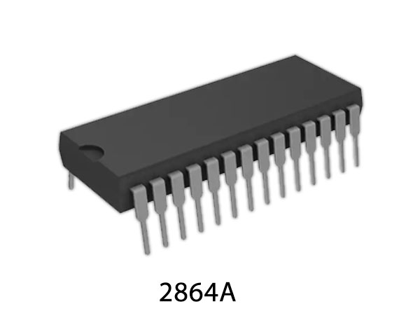
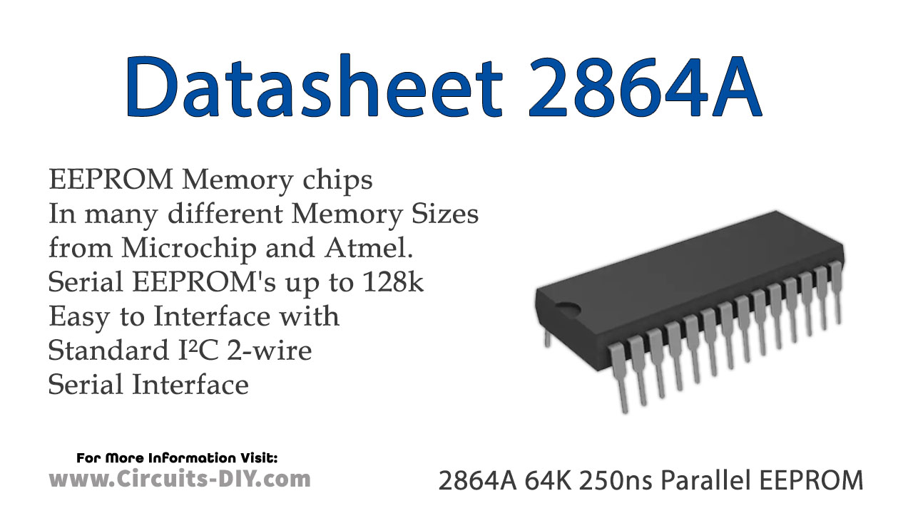
2864A Pinout
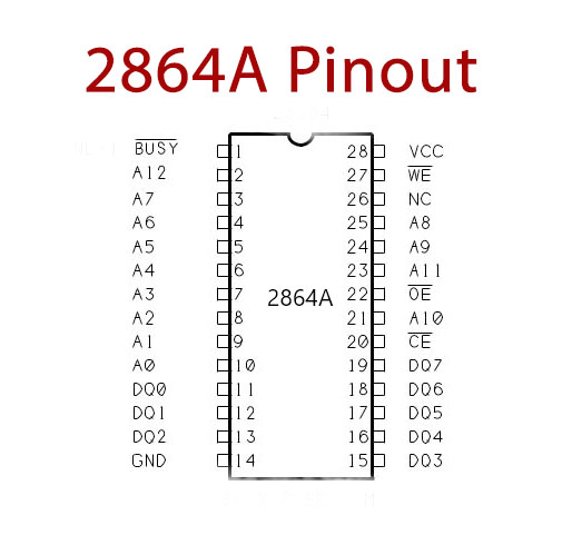
2864A Pin Configuration
| Pin No | Pin Name | Description |
| 1 | BUSY | Busy Pin |
| 2 | A12 | Address Pin 12 |
| 3 | A7 | Address Pin 7 |
| 4 | A6 | Address Pin 6 |
| 5 | A5 | Address Pin 5 |
| 6 | A4 | Address Pin 4 |
| 7 | A3 | Address Pin 3 |
| 8 | A2 | Address Pin 2 |
| 9 | A1 | Address Pin 1 |
| 10 | A0 | Address Pin 0 |
| 11 | DQ 0 | Data Inputs/Outputs 0 |
| 12 | DQ1 | Data Inputs/Outputs 1 |
| 13 | DQ 2 | Data Inputs/Outputs 2 |
| 14 | GND | Ground Pin |
| 15 | DQ 3 | Data Inputs/Outputs 3 |
| 16 | DQ 4 | Data Inputs/Outputs 4 |
| 17 | DQ 5 | Data Inputs/Outputs 5 |
| 18 | DQ 6 | Data Inputs/Outputs 6 |
| 19 | DQ 7 | Data Inputs/Outputs 7 |
| 20 | CE’ | Chip Enable Pin |
| 21 | A10 | Address Pin 10 |
| 22 | OE’ | Output Enable |
| 23 | A11 | Address Pin 11 |
| 24 | A9 | Address Pin 9 |
| 25 | A8 | Address Pin 8 |
| 26 | NC | No Connection |
| 27 | WE’ | Write Enable Pin |
| 28 | VCC | Supply Voltage Pin |
2864A Key Feature
- 25-bit 1:1 or 14-bit 1:2 configurable registered buffer
- Supports SSTL_18 JEDEC specification on data inputs and outputs
- Supports LVCMOS switching levels on C0, C1 and RESET# inputs
- Low voltage operation
- VDD = 1.7V to 1.9
- Available in 96 BGA package
- Drop-in replacement for ICSSSTUF32866
- Green packages availabl
You can download this datasheet for 2864A 64K 250ns Parallel EEPROM – Datasheet from the link given below:


