Contents
hide
The 2114A is a 4096-bit Static Random Access Memory organized as 1024 words by 4-bits. It uses fully DC stable (static) circuitry throughout, in both the array and the decoding, therefore it requires no clocks or refreshing to operate. Data access is particularly simple since address setup times are not required. The data is read out nondestructively and has the same polarity as the input data. Common input/output pins are provided.

2114 Pinout
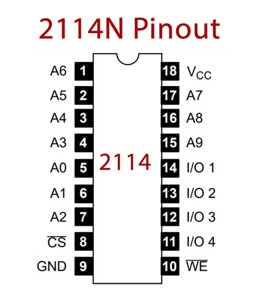
2114 Pin Configuration
| Pin No | Pin Name | Description |
|---|---|---|
| 1 | A6 | Address Pin 6 |
| 2 | A5 | Address Pin 5 |
| 3 | A4 | Address Pin 4 |
| 4 | A3 | Address Pin 3 |
| 5 | A0 | Address Pin 0 |
| 6 | A1 | Address Pin 1 |
| 7 | A2 | Address Pin 2 |
| 8 | CS’ | Chip Select Pin |
| 9 | GND | Ground Pin |
| 10 | WE’ | Write Enable Pin |
| 11 | I/O 4 | Data Inputs/Outputs 4 |
| 12 | I/O 3 | Data Inputs/Outputs 3 |
| 13 | I/O 2 | Data Inputs/Outputs 2 |
| 14 | I/O 1 | Data Inputs/Outputs 1 |
| 15 | A9 | Address Pin 9 |
| 16 | A8 | Address Pin 8 |
| 17 | A7 | Address Pin 7 |
| 18 | VCC | Power Supply Pin |
2114 Key Feature
- Vcc = 5V +- 5%
- GND = 0V
- Supply Current = 70mA max
- Read Cycle Time = 100ns min
- Access Time = 100ns max
- Chip Selection to Output Valid = 70ns max
- Write Cycle Time = 100ns min
- Write Time = 75ns min
- Write Release Time = 0ns min
- Output 3-state from Write = 30ns max
You can download this datasheet for 2114 1Kx4 200ns Low Power RAM – Datasheet from the link given below:


